|
|
|
 Schematic-driven PIC design process considering manufacturing tolerances
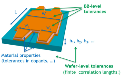
Inevitable manufacturing tolerances strongly degrade the fabrication yield of photonic integrated circuits (PICs), unless their effect on overall PIC performance characteristics is considered and mitigated during the PIC design process. This is especially true for PICs containing interferometric sub-circuits such as micro-ring optical filters, Mach-Zehnder interferometers, and arrayed waveguide gratings. The problem rapidly increases with the growth of complexity, which is currently observed while designing PICs for large-scale optical interconnects, LIDAR distribution networks, all-optical activation units for artificial neural networks, and multi-ring filters with complex custom transfer functions. Maximizing fabrication yield in such cases is a highly non-trivial task - it requires the development of special design approaches and easy access to statistical performance techniques during the simulations. We present a general-purpose schematic-driven PIC design framework that provides easy access to statistical performance techniques. Our design framework is based on statistical compact simulation models (CSMs) representing the photonic and optoelectronic building blocks (BBs) of foundry-specific process design kits (PDKs). We introduce a special technique that allows identifying critical light paths and applying automated phase compensation inside the models, which significantly simplifies the tolerances analysis, including estimating the final fabrication yield. The analysis of statistical parameter variations due to manufacturing tolerances on-waver and between wavers is supported as well by our presented approach. We demonstrate its application on complex PIC designs comprising of passive and active photonic building blocks.
Proc. of SPIE, Mar 2021.
|
 Virtual prototyping of complex photonic components and integrated circuits for polymer-based integration platform
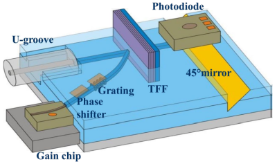
Recent developments in versatile polymer-based technologies and hybrid integration processes offer a flexible and cost-efficient alternative for creating very complex photonic components and integrated circuits. The fast and efficient test, optimization and verification of new ideas requires an automated and reproducible simulation and design process supporting flexible layout-driven and layout-aware schematic-driven methodologies. Targeting very complex designs, even small fabrication tolerances of one building block could make a huge difference on the performance and manufacturability of the whole structure. To reduce risk of failure and to make performance predictions by virtual prototyping reliable, the simulation model of each single building block needs to be working correctly based not only on the appropriate mathematical and physical equations, but also on adequate information provided by the foundry where the final structure will be manufactured.
The PolyPhotonics Berlin consortium targets to address these design challenges and establish a new versatile integration platform combining polymer with Indium-Phosphide and thin-film filter based technologies for numerous photonics applications in the global communications and sensing market. In this paper we will present our methodologies for modelling and prototyping optical elements including hybrid coupling techniques, and compare them with exemplary characterization data obtained from measurements of fabricated devices and test structures. We will demonstrate how the seamless integration between photonic circuit and foundry knowledge enable the rapid virtual prototyping of complex photonic components and integrated circuits.
Proc. of SPIE, Feb 2018.
|
 InP-based generic foundry platform for photonic integrated circuits
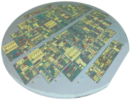
The standardization of photonic integration processes for InP has led to versatile and easily accessible generic integration platforms. The generic integration platforms enable the realization of a broad range of applications and lead to a dramatic cost reduction in the development costs of photonic integrated circuits (PICs). This paper addresses the SMART Photonics generic integration platform developments. The integration technology based on butt joint active-passive epitaxy is shown to achieve a platform without compromising the performance of the different components. The individual components or building blocks are described. A process design kit is established with a comprehensive dataset of simulation and layout information for the building blocks. Latest results on process development and optimization are demonstrated. A big step forward is achieved by applying high-resolution ArF lithography, which leads to increased performance for AWGs and a large increase in reproducibility and yield. The generic nature of the platform is demonstrated by analyzing a number of commercial multiproject wafer runs. It is clear that a large variety of applications is addressed with more than 200 designs from industry as well as academia. A number of examples of PICs are displayed to support this. Finally, the design flow is explained, with focus on layout-aware schematic-driven design flow that is required for complex circuits. It can be concluded that generic integration on InP is maturing fast and with the current developments and infrastructure it is the technology of choice for low cost, densely integrated PICs, ready for high-volume manufacturing.
IEEE J. Sel. Top. Quantum Electron., Jan/Feb 2018.
|
 Rapid virtual prototyping of complex photonic integrated circuits using layout-aware schematic-driven design methodology
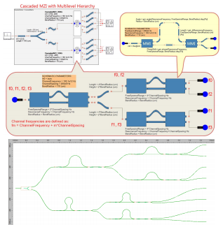
We present our versatile simulation framework for the schematic-driven and layout-aware design of photonic integrated circuits (PICs) realizing a fast and user-friendly design flow for large-scale PICs comprising passive and active building blocks (BBs). We show how the seamless interaction of circuit simulation with photonic layout design tools allows to specify and utilize directly physical locations and orientations of BBs of standardized process design kits (PDKs). We demonstrate how to combine graphical schematic capture and automated waveguide routing, and discuss by means of typical design applications how an optimized design flow can speed-up the virtual prototyping of complex PICs and optoelectronic applications.
Proc. of SPIE, Feb 2017.
|
 Layout-aware schematic-driven design methodology for photonic integrated circuits
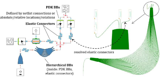
We introduce here a novel layout-aware schematic-driven PIC design methodology: a
circuit-level simulator supports the capability to specify directly physical locations and
orientations of PDK building blocks (BBs) on the final layout (when required by DRC
and packaging specifications or layout optimization) and to connect sub-circuits having
fixed locations by smart elastic optical connectors. This allows combining graphical
schematic capture and automated waveguide routing, which are currently considered
separately representing a major problem for PIC designers. Key enabler for this
functionality is the seamless integration of circuit and layout tools: a circuit simulator
automatically and invisibly for users invokes a layout design tool to determine the
actual physical lengths and shapes of all elastic connectors, constructs compact
simulation models for them, and after that initiates the circuit simulations.
Proc. Eur. Conf. Integr. Opt., May 2016.
|
 Purcell effect and Lamb shift as interference phenomena
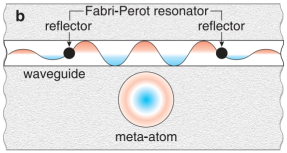
The Purcell effect and Lamb shift are two well-known physical phenomena which are usually discussed in the context of quantum electrodynamics, with the zero-point vibrations as a driving force of those effects in the quantum approach. Here we discuss the classical counterparts of these quantum effects in photonics, and explain their physics trough interference wave phenomena. As an example, we consider a waveguide in a planar photonic crystal with a side-coupled defect, and demonstrate a perfect agreement between the results obtained on the basis of quantum and classic approaches and reveal their link to the Fano resonance. We find that in such a waveguide-cavity geometry the Purcell effect can modify the lifetime by at least 25 times, and the Lamb shift can exceed 3 half-widths of the cavity spectral line.
Scientific Reports, Feb 2016.
|
 Modeling and design framework for SDM transmission systems
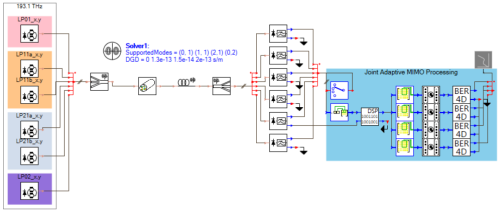
We present a sophisticated simulation framework for few-mode fiber based space division multiplexing (SDM) transmission systems supporting the characterization of the interplay between linear and nonlinear fiber effects, and design of key components such as optical amplifiers. We demonstrate its capabilities by discussing applications related to doped and un-doped multimode fiber design, linear and Kerr-induced mode coupling, and effective means for digital equalization at the receiver side.
Proc. ICTON, Jul 2015.
|
 Towards an automated design framework for large-scale photonic integrated circuits
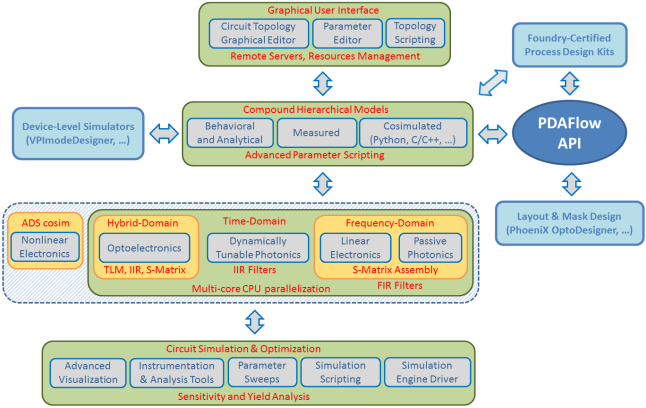
We present our approach towards an automated design framework for integrated photonics and optoelectronics, based on the experience of developing VPIcomponentMaker Photonic Circuits. We show that design tasks imposed by large-scale integrated photonics require introducing new "functional" types of model parameters and extending the hierarchical design approach with advanced parameter scripting capabilities. We discuss the requirements imposed by the need for seamless integration between circuit-level and device-level simulators, and illustrate our approach for the combination of VPIcomponentMaker Photonic Circuits and VPImodeDesigner. We show that accurate and scalable circuit-level modeling of large-scale photonic integrated circuits requires combination of several frequency- and time-domain simulation techniques (scattering-matrix assembly, transmission-line models, FIR and IIR digital filters, etc) within the same circuit simulation. We extend the scattering-matrix assembly approach for modeling linear electronic circuits, and motivate it being a viable alternative to the traditional modified nodal analysis approach employed in SPICE-like electronic circuit simulators. Further, we present our approach to support process design kits (PDK) for generic foundries of integrated photonics. It is based on the PDAFlow API which is designed to link different photonic simulation and design automation tools. In particular, it allows design and optimization of photonic circuits for a selected foundry with VPIcomponentMaker Photonic Circuits, and their subsequent export to PhoeniX OptoDesigner for layout verification and GDSII mask generation.
Proc. of SPIE, May 2015.
|
 The power of circuit simulations for designing photonic integrated circuits
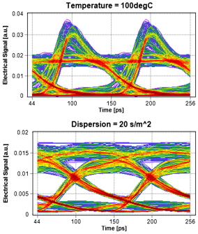
The emerging of circuit-level simulators for photonic integrated circuits (PICs) is driven by recent developments in technologies for integration of large-scale monolithic PICs in both, silicon and InP technologies. For that reason, powerful circuit-level simulators should be capable to model on the same circuit different types of sub-components performing photonic, electronic or opto-electronic, active or passive functions. In comparison with device-level simulations, the use of realistic circuit-level abstracted models facilitates rapid functional design without going into technological fabrication details and subsequent design flow. This accelerates the design process and decreases the number of runs to achieve the desired results. Detailed physical modeling remains limited to the design of some specific individual sub-elements. Large-scale PICs might comprise several thousands of elements. The circuit-level abstraction also ensures that the simulation speed to achieve a certain simulation accuracy decreases reasonably slowly with the total number of photonic components in the modeled PIC. In this work, we present our solution for modeling PICs in the framework of the circuit-level simulation tool VPIcomponentMaker Photonic Circuits (Carnotstr. 6, 10587, Berlin, Germany, www.VPIphotonics.com). We demonstrate the combination of different simulation approaches in time domain, frequency domain and time-and-frequency domain for fast and accurate simulations. We discuss several diverse modeling benefits by means of application examples on silicon photonic PICs.
Concurrency and Computation, Jul 2014.
|
 Parallel simulations of optical communication systems
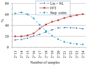
Sophisticated numerical simulations represent an indispensable tool for developing new optical communication systems and solutions. With wider availability of parallel computing hardware (most notably, multi-core CPUs and GPUs) it becomes increasingly important to effectively parallelize simulation algorithms. In this paper, we review the main principles and common pitfalls of parallel simulations for optical systems and components. The addressed topics include signal propagation in fibers, fiber gratings, active and passive semiconductor components, parallel simulations of transmission systems and photonic integrated circuits represented by networks of modules, as well as general-purpose optimization tasks.
Proc. of ICTON, Jul 2014.
|
 Modeling of opto-electronics in complex photonic integrated circuits

This work addresses a versatile modeling of complex photonic integrated circuits (PICs) including optical and electrical sub-elements. We introduce a new family of electrical elements, together with a novel electronic-photonic co-design, that complements current capabilities of photonic circuit simulators. This is illustrated with the modeling of complex electric circuits contained in photonic devices. Simulations of the interaction between electrical and optical parts allow the analysis of unwanted effects such as reflections due to impedance mismatching, as well as the optimization of the PIC as a whole. We illustrate the functionalities of our approach through application examples. As a use case, we present a model of the electrical driver for a monolithically-integrated InP transmitter developed in frame of the European research project MIRTHE and the analysis of the driver and the EA-Modulator interplay.
Proc. of SPIE, Mar 2014.
|
 Efficient design of photonic integrated circuits (PICs) by combining device- and circuit- level simulation tools
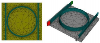 This work addresses a versatile modeling of complex photonic integrated circuits (PICs). We introduce a co-simulation solution for combining the efficient modeling capabilities of a circuit-level simulator, based on analytical models of PIC sub-elements and frequency-dependent scattering matrix (S-matrix) description, and an accurate electromagnetic field simulator that implements the finite element method (FEM) for solving photonic structures with complicated geometries. This is exemplified with the model of a coupled-resonator induced transparency (CRIT), where resonator elements are first modeled in the field simulator. Afterwards, the whole structure is created at a circuit level and statistical analysis of tolerances is investigated.
Proc. of SPIE, Mar 2013.
|
 Dual-time-scale simulation of dynamics and reconfiguration of fiber optical networks
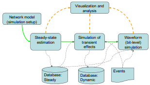 We describe an approach to simulate the power transients in complex (branched, ring, or mesh) transparent fiber optical networks. Simulations are performed at two time scales: first, the signal power dynamics in Erbium-doped fiber amplifiers is modeled at (sub-) millisecond scale using statistical signal descriptions. Further, the teletraffic performance of the network, such as the bit error rate, can be investigated for selected time instances at nano-second to sub-pico-second time scale using a sampled signal model ('bit-level' simulation). For the detailed simulation on 'bit-level', signal information and internal states of the network components are re-used form the first simulation step at (sub-) millisecond scale. To illustrate our approach, we discuss simulations of 'higher-order' transients in a ring network.
Proc. of ICTON, Jul 2012.
|
 Time-and-frequency-domain modeling (TFDM) of hybrid photonic integrated circuits
 This work addresses the efficient modeling of hybrid large-scale photonic integrated circuits (PICs) comprising both, active and passive sub-elements. We describe a new modeling approach, the time-and-frequency-domain modeling (TFDM) that improves accuracy, memory requirements and simulation speed in comparison with traditional pure timedomain method. In TFDM, clusters of connected linear PIC elements are modeled in frequency domain, while interconnections between such clusters and non-passive PIC elements are modeled in the time domain. Behavioral models of the fundamental building blocks of PICs are presented and combined in several application examples showing the robustness of the entire modeling framework for PICs.
Proc. of SPIE, Jan 2012.
|
 Detailed modeling of integrated IQ-transmitters for 100G+ applications
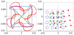 We present techniques for modeling the physics and systems-level characteristics of integrated IQ-transmitters for 100G+ applications and emphasize important design aspects. Using time-and-frequency-domain modeling (TFDM) of Photonic Integrated Circuits (PIC), we present a detailed IQ-transmitter model based on the physics and setup of active and passive subcomponents. With this, we link characteristics of subcomponents (bending loss of waveguides, phase changes in MMI couplers, sweep-out time of EAMs) to systems-level characteristics of the integrated IQ-transmitter (extinction ratio, modulation bandwidth, chirp). Further, a behavioral transmitter model is introduced and utilized to assess electrical driving requirements (allowed jitter, noise, synchronization offset).
Proc. of SPIE, Jan 2012.
|
 Hybrid Time-and-Frequency-Domain approach for modeling photonic integrated circuits
 Modern simulators of photonic integrated circuits (PICs) employ either frequency-domain or time-domain approaches for system-level modeling of PICs. We critically examine limitations of both approaches that obstruct their usage for simulations of large-scale PICs, and suggest an efficient hybrid alternative. Within this new approach clusters of connected linear PIC elements are modeled in frequency domain, while interconnections between such clusters and non-passive PIC elements are modeled in time domain.
Proc. of NUSOD, Sep 2011.
|
 Comparison of XPM and XpolM-induced impairments in mixed 10G-100G transmission
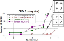 We reviewed the origin and impact of the cross polarization modulation (XpolM) effect. An analysis of the Manakov equation has been carried out in order to differentiate between XpolM and XPM effects. Based on this analysis, it has been argued that the impact of XpolM may have been overestimated so far. To verify this statement, the performance of a 112Gb/s DP-QPSK channel over 10Gb/s legacy system has been investigated with the help of numerical simulations. We showed that the impact of XpolM is smaller than the impact of XPM and intra-channel nonlinearities (iXPM, iFWM). Our presented results assessing the impact of the XpolM effect confirmed theoretical predictions that have been reported in. Finally, our investigations have shown that the impact of XpolM-induced distortion is reduced by PMD.
Proc. of ICTON, Jun 2011.
|
 Efficient design of Photonic Integrated Circuits
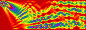 The exponentially growing number of components in complex large-scale Photonic Integrated Circuits (PICs) requires the necessity of photonic design tools with system-level abstraction. This work addresses the modeling of large-scale integrated PICs from a system-level perspective. Behavioral models of ring resonators, multimode interference devices, optical waveguides and other fundamental building blocks of PICs will be presented and combined to demonstrate several application examples of photonic circuit designs.
Proc. of ICTON, Jun 2011.
|
 Design of complex large-scale photonic integrated circuits (PICs) based on ring-resonator structures
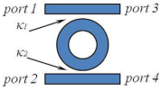 The exponentially growing number of components in complex large-scale Photonic Integrated Circuits (PICs) requires the necessity of photonic design tools with system-level abstraction, which are efficient for designs enclosing hundreds of elements. Ring-resonators and derived structures represent one example for large-scale photonics integration. Their characteristics can be parameterized in the frequency-domain and described by scattering matrix (S-matrix) parameters. The S-matrix method allows time efficient numerical simulations, decreasing the simulation time by several orders of magnitude compared to time-domain approaches yielding a better modeling accuracy as the number of PIC elements increases. We present the modeling of optical waveguides within a sophisticated design environment using application examples that contain ring-resonators as fundamental structure. In the models, the two orthogonally polarized guided modes are characterized by their specific index and loss parameters. Systematic variation of circuit parameters, such as coupling factor or refractive index, allows a comfortable design, analysis and optimization of many types of complex integrated photonic structures.
Proc. of SPIE, Jan 2011.
|
 Design of complex semiconductor integrated structures
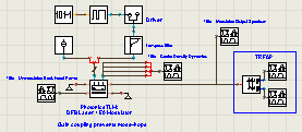 We present the benefits and limitations for designing complex optical semiconductor-based integrated structures by means of advanced numerical modeling. Multi-section tunable laser designs are presented and their tuning properties are analyzed for different architectures. We introduce a model of an integrated SOA with electroabsorption modulator. Its spectral properties are analyzed function of the parameters of the absorber section, showing the influence on the extinction ration of the generated signal. An InP-type Mach-Zehnder modulator is designed, illustrating the models of Kerr, Frank-Keldysh and QCSE effects. An example of a photo-detector demonstrates how dimensions and absorption parameters can be optimized to increase its detection bandwidth.
Proc. of SPIE, Nov 2009.
|
 Coupled-resonator-induced reflection in photonic-crystal waveguide structures
 We study the resonant transmission of light in a coupled-resonator
optical waveguide interacting with two nearly identical side
cavities. We reveal and describe a novel effect of the coupled-resonator-induced
reflection (CRIR) characterized by a very high and easily tunable
quality factor of the reflection line, for the case of the inter-site coupling
between the cavities and the waveguide. This effect differs sharply from the
coupled-resonator-induced transparency (CRIT) - an all-optical analogue
of the electromagnetically-induced transparency - which has recently been
studied theoretically and experimentally for the structures based on microring
resonators and photonic crystal cavities. Both CRIR and CRIT effects
have the same physical origin which can be attributed to the Fano-Feshbach
resonances in the systems exhibiting more than one resonance. We discuss
the applicability of the novel CRIR effect to the control of the slow-light
propagation and low-threshold all-optical switching.
Opt. Express, Jul 2008.
|
 Photonic crystals with anomalous dispersion: Unconventional propagating modes in the photonic band gap
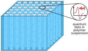 We present an investigation of the optical properties of photonic crystals whose constituent materials exhibit
anomalous dispersive behavior. In particular, the anomalous dispersion near resonances may lead to additional
propagating modes in the gap of the undoped system for a localized region of wave-vector space. Such a
system may be realized by infiltrating quantum dots in polymer suspensions into the pores of two-dimensional
high-index photonic crystals. An evaluation of the absorption lengths associated with these unconventional
modes and corresponding transmission calculations demonstrate that this effect can be observed in currently
accessible structures.
Phys. Rev. B, Jan 2008.
|
 Wannier-function based scattering-matrix formalism for photonic crystal circuitry
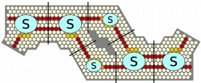 A guided-mode scattering matrix approach to photonic crystal integrated devices, based on the expansion of
the electromagnetic field in Wannier functions is presented and its applicability to large-scale photonic circuits
is demonstrated. In particular, we design two components typically used in wavelength division multi/demultiplexing applications, namely, a directional coupler and a Mach-Zehnder interferometer, and we analyze
the transmission spectra as a function of the coupler length and/or delay line length, respectively. These
examples demonstrate that by cascading basic functional elements, large-scale circuits can be accurately described
and efficiently designed with minimal numerical effort.
J. Opt. Soc. Am. B, Jan 2008.
|
 Low-threshold bistability of slow light in photonic-crystal waveguides
 We analyze the resonant transmission of light through a
photonic-crystal waveguide side coupled to a Kerr nonlinear cavity, and
demonstrate how to design the structure geometry for achieving bistability
and all-optical switching at ultralow powers in the slow-light regime. We
show that the resonance quality factor in such structures scales inversely
proportional to the group velocity of light at the resonant frequency
and thus grows indefinitely in the slow-light regime. Accordingly, the
power threshold required for all-optical switching in such structures scales
as a square of the group velocity, rapidly vanishing in the slow-light regime.
Opt. Express, Sep 2007.
|
 Periodic nanostrutures for photonics
 Periodic nanostructures in photonics facilitate a far-reaching control of light propagation and light-matter interaction. This article
reviews the current status of this subject, including both recent progress and well-established results. The primary focus is on the
basic physical principles and potential applications associated with the existence of Bragg scattering, photonic band structures, and
engineered effective-medium properties in periodic dielectric and metallo-dielectric systems. In addition, we discuss advantages
and limitations of various theoretical and numerical approaches as well as of those fabrication techniques that have specifically been
developed for this field.
Physics Reports, Mar 2007.
|
 All-optical switching, bistability, and slow-light transmission
in photonic crystal waveguide-resonator structures
 We analyze the resonant linear and nonlinear transmission through a photonic crystal
waveguide sidecoupled to a Kerr-nonlinear photonic crystal resonator. First, we extend the standard coupled-mode theory analysis to photonic crystal structures and obtain explicit analytical expressions
for the bistability thresholds and transmission coefficients which provide the basis for a detailed
understanding of the possibilities associated
with these structures. Next, we discuss limitations of standard coupled-mode theory and present an
alternative analytical approach based on the effective discrete equations derived using a Green's function
method. We find that the discrete nature of the photonic crystal waveguides allows a geometry-driven enhancement
of nonlinear effects by shifting the resonator location relative to the waveguide, thus providing an
additional control of resonant waveguide transmission and Fano resonances. We further demonstrate that this
enhancement may result in the lowering of the bistability threshold and switching power of nonlinear devices
by several orders of magnitude. Finally, we show that employing such enhancements is of paramount importance
for the design of all-optical devices based on slow-light photonic crystal waveguides.
Phys. Rev. E, Oct 2006.
|
 Wannier basis design and optimization of a photonic crystal
waveguide crossing
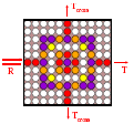 The Wannier functions approach is very efficient by itself...
But in combination with the small-rank inverse matrix adjustment
it becomes an extremely powerful tool for the usually
computationally very demanding problem of
device optimization. Here, we demonstrate
its power by designing a highly efficient
non-resonant broadband
low-cross-talk waveguide intersection which is fairly stable
with respect to the fabrication imperfections.
The calculations on a regular personal computer took about
3-5 seconds per design realization what permitted us to check all
possible alternatives.
IEEE Photonics Technol. Lett., Sep 2005.
|
 Nonlinear Fano resonance and bistable wave transmission
 Here, we study both,
linear and nonlinear, transmission of continuous waves and
gaussian pulses for several modifications of a discrete
Fano-Anderson model with the waveguide coupled to a
single nonlinear defect. We obtain a number
of explicit analytical results
which allow one to get a deeper understanding of the physics
of this phenomenon.
Phys. Rev. E, Mar 2005.
|
 Tunable photonic crystal circuits: concepts and designs based
on single-pore infiltration
 Here, we demonstrate that the infiltration of individual pores
of certain two-dimensional photonic crystals with low-refractive index
materials (liquid crystals or polymers) provides an efficient
platform for the realization of integrated photonic crystal
circuitry. As an illustration, we present designs for monomode
photonic crystal waveguides with efficient designs for waveguide
bends, beam splitters, and waveguide intersections.
Opt. Lett., Dec 2004.
|
 Arbitrary angle waveguiding applications of two-dimensional
curvilinear-lattice photonic crystals
 In the case of artificially
manufactured PBG materials there are no strict principal
limitations inherent for atomic and molecular crystals and
quasi-crystals, and potentially the employed structures of
PBG materials can have quite sophisticated types of
ordering.
In this Letter we introduce a novel sub-class of PBG
materials, which we call curvilinear-lattice
photonic crystals. We demonstrate the existence
of a robust photonic band gap in such structures and
discuss their possible applications.
Appl. Phys. Lett., Jun 2004.
|
 Band-gap engineering and defect modes in photonic crystals
with rotated hexagonal holes
 Here, we
explore further the concept of the enlargement of the
absolute band gaps of 2D photonic crystals through
reducing symmetry in the unit-cell geometry, e.g.,
using rotated hexagonal holes. We demonstrate that
by rotating such hexagonal holes it is possible to
slightly tune the localized defect modes - such a
tunability is important for designing
waveguides that would be able to
efficiently guide light of both polarizations.
Laser Physics, May 2004.
|
 The Wannier function approach to photonic crystal circuits
(Topical Review)
 We introduce a novel approach to the accurate and efficient calculation
of the optical properties of defect structures embedded in photonic
crystals (PCs). This approach is based on an expansion of the
electromagnetic field into optimally adapted photonic Wannier functions,
which leads to effective lattice models of the PC structures.
J. Phys.: Condens. Matter, Sep 2003.
|
 Scattering matrix approach to large-scale photonic crystal circuits
 Which approach is the most efficient for modelling large-scale
photonic crystal circuits? We suggest here that it is a scattering
matrix approach with S-matrices expressed in the basis
of guided modes of photonic crystal waveguides instead of
commonly used basis of plane waves.
Opt. Lett., Apr 2003.
|
 Nonlinear transmission and light localization in photonic-crystal waveguides
 Here, we apply the discrete equations with long-range interactions
(which we have
derived previousely)
to the case of nonlinear defects
embedded into 2D photonic crystals. We demonstrate that such
nonlinear defect structures
can be used for creation of all-optical switching devices, optical
isolators, optical limiters, and other functional devices for photonic
integrated circuits.
J. Opt. Soc. Am. B, Sep 2002.
|
 Nonlinear Photonic Crystals: Toward All-Optical Technologies
 Many of us believe that nonlinear photonic crystals offer
an opportunity to create
the all-optical analogs of diodes and transistors that will
one day enable the first all-optical computer to be built.
Here, we dream about a little bit more specifically...
Opt. Photon. News, Jul 2002.
|
|
|

