|
|
|
|
| Recent Work (2014 - 2024): |
Product and Project Manager for the development of
VPIdeviceDesigner™
–
a versatile simulation framework for the analysis and optimization of integrated photonic devices, waveguides, and optical fibers.
This powerful design tool offers a set of full-vectorial finite-difference mode solvers for waveguide analysis as well as a beam propagation method (BPM) and an eigenmode expansion method (EME) for simulating 2D and 3D photonic devices.
VPIdeviceDesigner supports the flexible definition of 2D waveguide cross-sections and 3D device layouts with realistic (dispersive, temperature-dependent, etc.) optical materials and widely customizable nonuniform meshing.
VPIdeviceDesigner provides a user-friendly object-oriented Python interface, which is closely integrated with the Python-based ecosystem of open-source software for mathematics, science, and engineering, including the libraries NumPy, SciPy, and the comprehensive 2D plotting library Matplotlib.
Besides, VPIdeviceDesigner facilitates the easy creation of compact simulation models for the designed waveguides and devices, enabling seamless integration with VPIcomponentMaker Photonic Circuits and its VPItoolkit PDK extensions.

| Recent Work (2010 - 2023): |
Product and Project Manager for the development of
VPIcomponentMaker™ Photonic Circuits
–
an accurate and fast EDA-style simulation and design environment for elaborating modern and next generation photonic integrated circuits (PICs).
Such PICs are large-scale and heterogeneous, consisting of hundreds (many thousands in a few years) of passive photonic, active optoelectronic, and electronic elements. For their modeling, VPIcomponentMaker Photonic Circuits supports scalable heterogeneous circuit-level simulation framework: time- and frequency-domain simulation domains are seamlessly merged and can, therefore, be combined within the same modeled circuit.
| Recent Work (2015 - 2023): |

|
 Schematic-driven PIC design process considering manufacturing tolerances
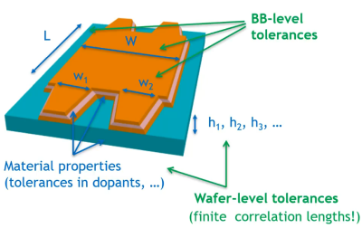
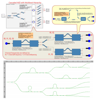
Inevitable manufacturing tolerances strongly degrade the fabrication yield of photonic integrated circuits (PICs), unless their effect on overall PIC performance characteristics is considered and mitigated during the PIC design process. This is especially true for PICs containing interferometric sub-circuits such as micro-ring optical filters, Mach-Zehnder interferometers, and arrayed waveguide gratings. The problem rapidly increases with the growth of complexity, which is currently observed while designing PICs for large-scale optical interconnects, LIDAR distribution networks, all-optical activation units for artificial neural networks, and multi-ring filters with complex custom transfer functions. Maximizing fabrication yield in such cases is a highly non-trivial task - it requires the development of special design approaches and easy access to statistical performance techniques during the simulations. We present a general-purpose schematic-driven PIC design framework that provides easy access to statistical performance techniques. Our design framework is based on statistical compact simulation models (CSMs) representing the photonic and optoelectronic building blocks (BBs) of foundry-specific process design kits (PDKs). We introduce a special technique that allows identifying critical light paths and applying automated phase compensation inside the models, which significantly simplifies the tolerances analysis, including estimating the final fabrication yield. The analysis of statistical parameter variations due to manufacturing tolerances on-waver and between wavers is supported as well by our presented approach. We demonstrate its application on complex PIC designs comprising of passive and active photonic building blocks.
Proc. of SPIE, Mar 2021.
|
Virtual prototyping of complex photonic components and integrated circuits for polymer-based integration platform
Recent developments in versatile polymer-based technologies and hybrid integration processes offer a flexible and cost-efficient alternative for creating very complex photonic components and integrated circuits. The fast and efficient test, optimization and verification of new ideas requires an automated and reproducible simulation and design process supporting flexible layout-driven and layout-aware schematic-driven methodologies. Targeting very complex designs, even small fabrication tolerances of one building block could make a huge difference on the performance and manufacturability of the whole structure. To reduce risk of failure and to make performance predictions by virtual prototyping reliable, the simulation model of each single building block needs to be working correctly based not only on the appropriate mathematical and physical equations, but also on adequate information provided by the foundry where the final structure will be manufactured.
The PolyPhotonics Berlin consortium targets to address these design challenges and establish a new versatile integration platform combining polymer with Indium-Phosphide and thin-film filter based technologies for numerous photonics applications in the global communications and sensing market. In this paper we will present our methodologies for modelling and prototyping optical elements including hybrid coupling techniques, and compare them with exemplary characterization data obtained from measurements of fabricated devices and test structures. We will demonstrate how the seamless integration between photonic circuit and foundry knowledge enable the rapid virtual prototyping of complex photonic components and integrated circuits.
Proc. of SPIE, Feb 2018.
|
InP-based generic foundry platform for photonic integrated circuits
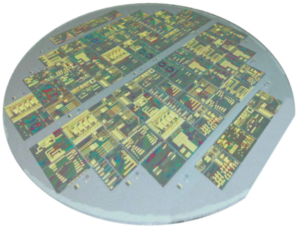
The standardization of photonic integration processes for InP has led to versatile and easily accessible generic integration platforms. The generic integration platforms enable the realization of a broad range of applications and lead to a dramatic cost reduction in the development costs of photonic integrated circuits (PICs). This paper addresses the SMART Photonics generic integration platform developments. The integration technology based on butt joint active-passive epitaxy is shown to achieve a platform without compromising the performance of the different components. The individual components or building blocks are described. A process design kit is established with a comprehensive dataset of simulation and layout information for the building blocks. Latest results on process development and optimization are demonstrated. A big step forward is achieved by applying high-resolution ArF lithography, which leads to increased performance for AWGs and a large increase in reproducibility and yield. The generic nature of the platform is demonstrated by analyzing a number of commercial multiproject wafer runs. It is clear that a large variety of applications is addressed with more than 200 designs from industry as well as academia. A number of examples of PICs are displayed to support this. Finally, the design flow is explained, with focus on layout-aware schematic-driven design flow that is required for complex circuits. It can be concluded that generic integration on InP is maturing fast and with the current developments and infrastructure it is the technology of choice for low cost, densely integrated PICs, ready for high-volume manufacturing.
IEEE J. Sel. Top. Quantum Electron., Jan/Feb 2018.
|
Rapid virtual prototyping of complex photonic integrated circuits using layout-aware schematic-driven design methodology
We present our versatile simulation framework for the schematic-driven and layout-aware design of photonic integrated circuits (PICs) realizing a fast and user-friendly design flow for large-scale PICs comprising passive and active building blocks (BBs). We show how the seamless interaction of circuit simulation with photonic layout design tools allows to specify and utilize directly physical locations and orientations of BBs of standardized process design kits (PDKs). We demonstrate how to combine graphical schematic capture and automated waveguide routing, and discuss by means of typical design applications how an optimized design flow can speed-up the virtual prototyping of complex PICs and optoelectronic applications.
Proc. of SPIE, Feb 2017.
|
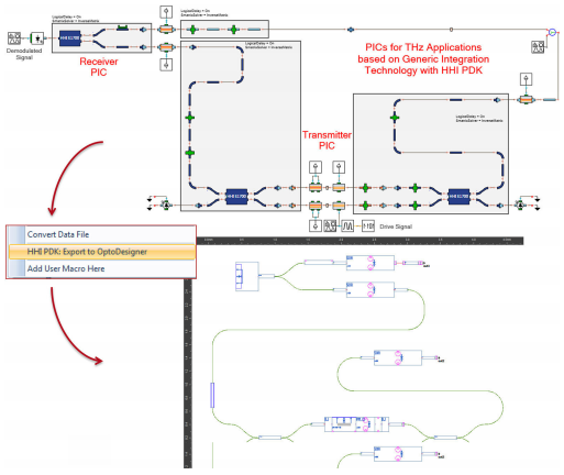
Layout-aware schematic-driven design methodology for photonic integrated circuits
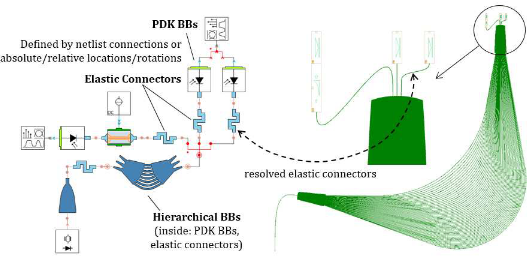
We introduce here a novel layout-aware schematic-driven PIC design methodology: a
circuit-level simulator supports the capability to specify directly physical locations and
orientations of PDK building blocks (BBs) on the final layout (when required by DRC
and packaging specifications or layout optimization) and to connect sub-circuits having
fixed locations by smart elastic optical connectors. This allows combining graphical
schematic capture and automated waveguide routing, which are currently considered
separately representing a major problem for PIC designers. Key enabler for this
functionality is the seamless integration of circuit and layout tools: a circuit simulator
automatically and invisibly for users invokes a layout design tool to determine the
actual physical lengths and shapes of all elastic connectors, constructs compact
simulation models for them, and after that initiates the circuit simulations.
Proc. Eur. Conf. Integr. Opt., May 2016.
|
Purcell effect and Lamb shift as interference phenomena
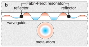
The Purcell effect and Lamb shift are two well-known physical phenomena which are usually discussed in the context of quantum electrodynamics, with the zero-point vibrations as a driving force of those effects in the quantum approach. Here we discuss the classical counterparts of these quantum effects in photonics, and explain their physics trough interference wave phenomena. As an example, we consider a waveguide in a planar photonic crystal with a side-coupled defect, and demonstrate a perfect agreement between the results obtained on the basis of quantum and classic approaches and reveal their link to the Fano resonance. We find that in such a waveguide-cavity geometry the Purcell effect can modify the lifetime by at least 25 times, and the Lamb shift can exceed 3 half-widths of the cavity spectral line.
Scientific Reports, Feb 2016.
|
Modeling and design framework for SDM transmission systems
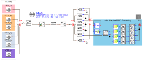
We present a sophisticated simulation framework for few-mode fiber based space division multiplexing (SDM) transmission systems supporting the characterization of the interplay between linear and nonlinear fiber effects, and design of key components such as optical amplifiers. We demonstrate its capabilities by discussing applications related to doped and un-doped multimode fiber design, linear and Kerr-induced mode coupling, and effective means for digital equalization at the receiver side.
Proc. ICTON, Jul 2015.
|
Towards an automated design framework for large-scale photonic integrated circuits
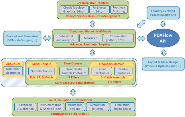
We present our approach towards an automated design framework for integrated photonics and optoelectronics, based on the experience of developing VPIcomponentMaker Photonic Circuits. We show that design tasks imposed by large-scale integrated photonics require introducing new "functional" types of model parameters and extending the hierarchical design approach with advanced parameter scripting capabilities. We discuss the requirements imposed by the need for seamless integration between circuit-level and device-level simulators, and illustrate our approach for the combination of VPIcomponentMaker Photonic Circuits and VPImodeDesigner. We show that accurate and scalable circuit-level modeling of large-scale photonic integrated circuits requires combination of several frequency- and time-domain simulation techniques (scattering-matrix assembly, transmission-line models, FIR and IIR digital filters, etc) within the same circuit simulation. We extend the scattering-matrix assembly approach for modeling linear electronic circuits, and motivate it being a viable alternative to the traditional modified nodal analysis approach employed in SPICE-like electronic circuit simulators. Further, we present our approach to support process design kits (PDK) for generic foundries of integrated photonics. It is based on the PDAFlow API which is designed to link different photonic simulation and design automation tools. In particular, it allows design and optimization of photonic circuits for a selected foundry with VPIcomponentMaker Photonic Circuits, and their subsequent export to PhoeniX OptoDesigner for layout verification and GDSII mask generation.
Proc. of SPIE, May 2015.
|
|
|
|